| Objectives: To present basic characteristic and limitations of gates. |
Topics covered:
Digital logic is implemented using integrated circuits which are classified into families based on their basic electronic structure. A common structure is the bipolar transistor/transitor logic (TTL) which you will be using in the laboratory. Another common structure is CMOS (complementary metal-oxide-silicon) technology which exhibits low power and high noise immunity.
Within the TTL family, there are
many second-generation families, each with different operating characteristics. Two important factors in the consideration
of each logic family are speed and power consumption. These two tend to be directly related, i.e., higher speed
consumes more power. Families can be characterized by the relationship between propagation-delay and power. The
chart shows the speed-power relationship of common TTL families.
Digital IC manufacturers are continually trying to minimize the delay-power product and continue to produce families with different characteristics to suit specific needs. The following table is a growing list of various sub-families with their characteristics and designations
| Family | Characteristics | Example |
| TTL | Standard transistor/transistor logic | 7400 |
| L | Low power TTL | 74L00 |
| H | High speed TTL | 74H00 |
| S | Schottky TTL - high speed | 74S00 |
| LS | Low power Schottky TTL | 74LS00 |
| AS | Advanced Schottky | 74AS00 |
| ALS | Advanced Low power Schottky | 74ALS00 |
| F | Fast Schottky | 74F00 |
| HC | High speed CMOS | 74HC00 |
| HCT | High speed CMOS, TTL-voltage compatible | 74HCT00 |
| AC | Advanced CMOS | 74AC00 |
| ACT | Advanced CMOS, TTL-output compatible | 74ACT00 |
In order to put into perspective where the above devices fit into the scheme of things and how far we have come, it would be instructive to look at a chronology of computer electronics.
1906 - Vacuum tube invented by Lee De Forest.
1946 - The ENIAC digital computer built, 18 feet high x 80 feet long, with 17,000 tubes.
1947 - Transistor invented by William Shockley.
1955-1965 - Discrete transistor usage increases.
1958 - Integrated circuit invented by Jack Kilby.
1960 - ICs proliferate
SSI - Small scale integration - >10 transistors (1 to 30 gates)
MSI - Medium scale integration - >100 transistors (10 to 300 gates)
LSI - Large scale integration - >1000 transistors (100 to 3000 gates)
1971 - Intel 4004 microprocessor, with 2,250 transistors.
1978 - VLSI - Very large scale integration, >10,000 transistors (1000 - 30,000 gates)
1979 - Motorola 68000 microprocessor, 70,000 transistors.
1985 - ASICs (application-specific ICs) appear with >100,000 gates.
1995 - CPU, memory functions available in ASICs with >1 million gates.
Reference: Understanding Computers, Time-Life Books.
If you examine a typical circuit board today you will find more use of large ICs with hundreds of pins and fewer
7400 style ICs.
Usage of discrete SSI and MSI functions such as gates, flip-flops and registers have decreased over the years. Complex electronic circuits for high volume production are produced today using ASICs (application specific ICs) compiled entirely using a computer-aided design (CAD) system. The design engineer selects all gates and logic functions which may also include a CPU and RAM. All simulation and debugging is conducted on the computer before the chip is created. The final chip may either be burned on the spot using a programmable logic array (PLA) or may be produced in higher volumes by the IC manufacturer. Regardless of the IC's complexity or how it is created, basic knowledge of gates and flip-flops is still essential.
The schematic of a typical TTL 7400 NAND gate is shown in Figure 6.2.
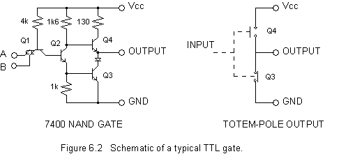
In this diagram, observe that the output stage consists of two active elements, Q3 and Q4. This circuit is designed such that the operation of Q3 and Q4 are complementary, that is, when one transistor is ON the other is OFF. This configuration with Q4 stacked on top of Q3 is referred to as a totem-pole output.
Also shown in Figure 6.2 is a simplified schematic of the operation of the totem-pole output. Transistors Q3 and Q4 behave as switches controlled by the INPUT. At any time, only one of the two switches is closed while the other is open. In other words, when Q3 is closed, Q4 is open. Conversely, when Q3 is open, Q4 is closed. By analyzing this circuit you can follow how the OUTPUT changes from 0 to 5 volts.
Figure 6.3 shows the schematic of a typical TTL gate with open-collector output, for example, a 7403 NAND gate. Observe here that the circuit elements associated with Q4 in the totem-pole circuit are missing and the collector of Q3 is left open-circuited, hence the name open-collector.
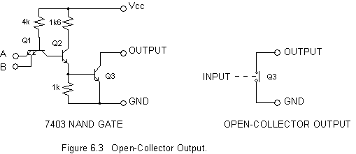
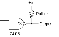 An open-collector output has current sinking
capabilities, that is, it can present a logic-LO output. In contrast with a normal totem-pole output, it cannot
be the source of current and therefore cannot present a logic-HI on its own. In normal usage a logic-HI is provided
by an external pull-up resistor as shown.
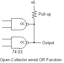 Outputs of several open-collector gates
may be directly wired together to form a wired-OR logic function for negative logic. This is useful
for creating a party-line data bus or control bus whereby any one of several circuits may pull the
line LO without causing damage to another active output. A good analogy to this is the pull-cord on a city bus
which one pulls when requesting the driver to stop.
Boolean logic is based on a binary system whereby an output can have one of two states, ON or OFF. What is meant by tri-state or 3-state outputs? Let us examine the typical totem-pole output once again.
|
Q4 |
Q3 |
OUTPUT |
|
OFF |
ON |
0 |
|
ON |
OFF |
1 |
|
OFF |
OFF |
HI-Z |
|
ON |
ON |
DAMAGING |
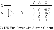 This third state is a useful feature
and is employed in tri-state outputs as another way of creating party-line bus systems. The 74126 tri-state bus
driver has an enable input G. When G is LO, the output is in the high impedance state. When G is active
(HI), the gate is enabled and the output is a normal TTL level. Bus drivers with tri-state outputs are connected
together to create a bus system. Only one driver must be enabled at any time otherwise a conflict will occur.
| Objectives: To give students a sense of the magnitudes of voltage, current, resistance, capacitance, time, frequency, etc. encountered in electronics. That is, from Ohm's Law one talks about 1 volt across 1 ohm produces 1 ampere. In digital electronics, typical resistances are 100 to 10K-ohm, currents are 10µA to 10mA, capacitances are 100pF to 1µF. |
 All inputs to logic gates must
be connected to logic LO or HI. An unconnected input is said to be floating. Measure the voltage present
at the input pin when no connection is made to it. Does this input constitute a logic LO or logic HI input?
Inputs to TTL gates may experience voltages ranging from 0 to 5 volts. What is the voltage range that would be considered a logic LO? What is the range that would be considered a logic HI?
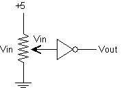 Draw the input/output transfer
characteristics of a 7404 inverter. Use a 1K potentiometer to supply a variable input voltage. Measure both
the input voltage and the logic output of the inverter. Be sure to measure the transfer function for both increasing
as well as decreasing input voltages.
Repeat the above exercise using a 7414 Schmitt trigger.
The inputs of logic gates present loads within a circuit. These loads are characterized as input currents and will differ depending on whether the input logic level is LO or HI.
 (a)
Measure the input voltage and determine the HI-level input current IIH
of a typical gate of the 74xx or 74LSxx TTL families. Compare your results with
the specifications in the TTL Data Book
from the IC manufacturer.
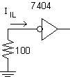 (b)
Measure the input voltage and determine the LO-level current IIL
of a 74xx or 74LSxx TTL gate. Compare your results with the specifications in
the TTL Data Book.
TTL totem-pole outputs are designed to drive loads both LO and HI. The HI-level output current IOH is a measure of how well the output can drive loads HI.
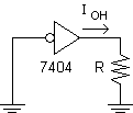 (a) Apply a load of R = 1K ohms
and measure the HI-level output voltage. What is the HI-level output current IOH for that gate? What
is the lowest value of R such that the output is still HI?
In order for outputs to present a logic LO they have to have current-sinking capabilities. The LO-level output
current IOL is a measure of how well the output can sink current.
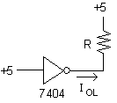 (b) With a pull-up load of
R = 220 ohms, measure the LO-level output voltage. What is the LO-level output current IOL for this
gate? What is the smallest value of R such that the output is still LO?
 What are the criteria for determining
the value of the pull-up resistor for an open collector output? Calculate the range of values for this resistor.
Do this before looking at the solution in the TTL Data Book for maximum and minimum R.
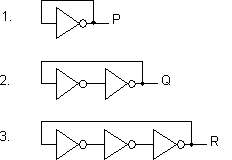 The propagation delay inherent
in gates can be useful for creating oscillatory circuits. Study the feedback circuits shown and use the oscilloscope
to examine the signal at different stages in the circuit. Analyze the circuits and explain the results. From the
measurements taken determine the propagation delay of a typical 7404 gate. (74LS04
Data Sheet)
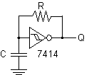 Construct this simple oscillator
and measure the frequency of oscillation for a given R and C.
The 555 timer IC is a popular circuit for generating asymmetric rectangular waves. Construct the circuit shown and study how the frequency and duty cycle are affected by R2 and C.
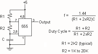
 Using
a very high frequency clock input measure the propagation delay of a
typical 74xx or 74LSxx TTL gate. Measure both LO-to-HI (tPLH) and
HI-to-LO (tPHL) propagation delays and compare your results with
the specifications given in the TTL
Data Book.
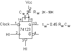 The circuit shows one-half
of a 74LS123 dual "one-shot" monostable multivibrator being
used to generate a pulse of adjustable width. Construct and test this circuit. Draw the input and output waveforms
(timing diagram).
What is the minimum pulse width?
What happens if the pulse width tW exceeds the period tC of the input clock?
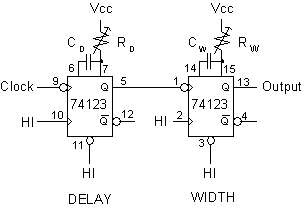 A common requirement in nuclear
radiation counting systems is a circuit which will delay and reshape the voltage pulse originating from a detector.
A pair of "one-shots" is used to generate a pulse of width tW that occurs at a delayed time
tD after the trigger event. Construct and test this circuit and draw the timing diagram.