|
|||
|
Tech
Talk
|
|||
|
Printed
Circuit Boards (PCB)
|
Want to make your own printed circuit boards? Yes you can. I have done it for years. There are short cuts, special pens or special paper available that allow you to iron on the pattern to a pre-sensitized copper laminate. The end result is not as good as doing it the proper way. So what is the proper way? Briefly, here are the steps required in making a PCB.
1. Make a black and white print, or black on transparent film
layout of the board design. (This is best done at twice life size).
2. Make a photographic negative on film of the design, life size.
3. Scrub and clean a blank sheet of copper laminate, single or double sided
as desired. Coat the copper sides with photo resist and leave to dry (done
in a photography darkroom).
4. Sandwich the board between the negative films (if double sided) and expose
to UV light (best done using a vacuum easel).
5. Develop the etch resist with photo resist developer and wash with hot water.
6. Etch the board in a hot bubbling bath of etching solution (done in a fume
hood). The traditional solution of ferric chloride is very nasty stuff. A
solution that is less pungent is ammonium persulphate.
7. Finally, drill your component holes using high speed carbide drills.
Sounds like a lot of work? Believe me, it is. Besides being time consuming,
you need the equipment, chemicals and facilities to do it. In today's internet
world there is a much easier way.
1. Draw your PCB design on your computer using any of many programs
available.
2. View and check your design
3. Send the layout files via the internet to a PCB fab.
4. Sit and wait 3 days for the finished boards to come back
Yes! It is that easy. It only costs you a little bit of money, but reasonably priced. I have been using Alberta Printed Circuits for years and I'm very pleased with their prototyping service.
What's so special about this service? Here are a few things to know.
1. Prototype boards are shipped the next business day. So it
takes 3 days to be delivered from the time you send in your order. If you
are in a rush you pay more bucks.
2. Basic service is double sided PCB with plated thru holes - no solder masks
(the green film that covers the whole board except the solder pads) and no
overlays (white silk screening that shows component placement, numbers and
other writing).
3. Boards are made in multiples of 2. Remember, this is only your prototype
so you shouldn't be planning on making 100 boards!
4. At the time of writing (Aug 2006) there is a CAN$55 setup charge and material
charge of about $1 per sq. inch. So as an example, two 4 x 5" boards
would cost just under $100 or $50 per board. Of course, the setup charge gets
amortized the more boards you make. For quantity of 10 boards, the cost would
drop to about $25 per board. This may still be expensive but remember this
is a prototype. For production runs you should shop around. Check out their
on-line Prototype Price Estimator to figure out the cost of your board.
5. Choose drill sizes from a standard free list at no extra charge. Pay an
extra $7 for every drill size that is not on the free list. In most cases,
there is usually no reason not to stick with the standard sizes.
6. On their web site is a wealth of information on making PCBs, well worth
reading.
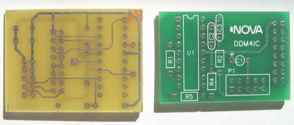
Sample prototype PCB is on the left, production board with green solder mask
and white overlay shown on the right.
Getting Started
OK. So how do you get started laying out the board design? The first step is to draw your circuit schematic. You can do this by hand on a sheet of paper or you can use a schematic drawing program. There are very good programs available on the internet.

If you are doing this for the first time, it might be a good idea to start with a rough design of your layout on paper. Get a pad of checkered paper (on ¼ inch grid spacing), a red and blue pencil crayon(or green or ordinary pencil) and eraser. Draw the layout you have in mind, with red traces for the top layer and blue for the bottom. This will give you a good idea on the size of your PCB and placement of components. You will save a lot of time ripping up and rerouting traces when you start working on the computer version of the layout.
The next step is to draw the board layout using a computer program. Eagle is an integrated schematic capture and board layout program. You can try out any one of these.
Eagle from www.cadsoftusa.com
Circuit Maker by Microcode (now owned by Altium) www.altium.com
Protel EasyTrax (freeware)
I prefer to use EasyTrax from Protel (now owned by Altium). This is available on the Alberta Printed Circuits web site.
www.apcircuits.com/resources/downloads/downloads.html
You create the PCB design using EasyEdit. Once you are finished, you use EasyPlot to create the numeric control (NC) machine files, called Gerber files which will be sent to the fab shop with your order. But before you send the files off, it is advisable… correction … you must view the Gerber files on a viewer and double check that every thing is ok. You can print out the layout in colour using the viewer. Pentalogix ViewMate is also available at www.apcircuits.com
There are a few hiccups in every step along the way, which I will document at a later date. If you encounter problems, feel free to contact me and I will assist you.
$$$ site under construction $$$
Things to add:
Pads
SMD pads
Ground planes
Decoupling capacitors
Laying last traces
Jumpers
0-ohm jumpers
Layout tips
2006.08.28