|
Femtosecond laser micromachining is a rapidly advancing area
of deployment for ultrashort pulse lasers. It has been shown
that optical pulses of femtosecond duration offer many advantages
in the selective ablation and modification of materials. In
linearly absorbing materials, collateral damage can be largely
avoided. Moreover, femtosecond optical pulses in the linear
transmission band of a material can be used to modify materials
in sub-surface regions. In this case, multiphoton processes
can be employed at the laser focus to deposit energy in a
selective and spatially well-defined manner.
 Femtosecond Laser Ablation and Micromachining Setup Femtosecond Laser Ablation and Micromachining Setup |
In our research we use the following laser systems:
| Laser | Rep. Rate | Max. Pulse Energy | Wavelength [nm] | Pulse Width |
| Ti:sapphire Oscillator | ~80 MHz | 10 nJ | 760 - 840 | 90 fs |
| Ti:sapphire Amplifier | 1 Hz - 1kHz | 0.4 mJ | 760 - 840 | ~ 130 fs |
| Ti:sapphire Amplifier | 1 Hz - 1kHz | 1.0 mJ | 800 | ~ 50 fs |
| OPA signal | | 90 µJ | 1100 - 1600 nm | 50 - 100 fs |
| OPA idler | | 30 µJ | 1600 - 3000 nm | 50 - 100 fs |
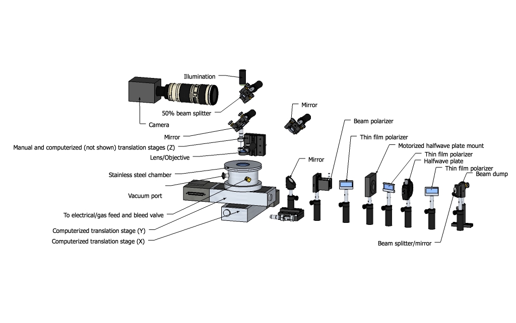
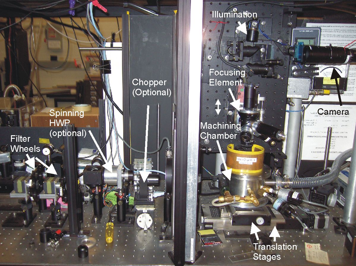
A schematic diagram and a photograph of our laser micromachining setup are shown below. (Click to enlarge the images.)
| Our Research |
We study the advantages and feasibility of using
femtosecond pulses for direct writing, cutting, drilling and
modification of a wide variety of materials, such as semiconductors,
metals, dielectrics and thin films. In our studies we concentrate
on detailed post mortem analysis of the material after femtosecond
irradiation. The final state of the material has been characterized
by using scanning electron microscopy (SEM), transmission electron
microscopy (TEM) along with focussed ion beam (FIB) techniques,
atomic force microscopy (AFM), and optical techniques.
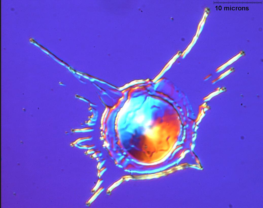
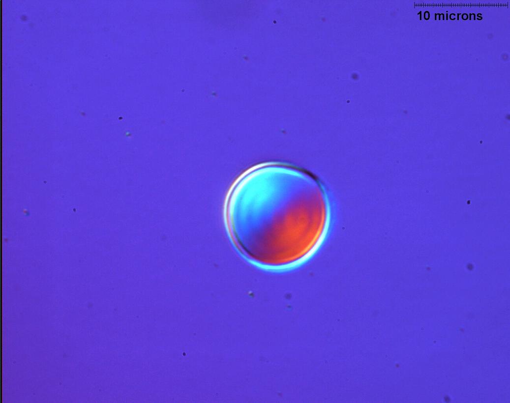
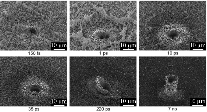
| Single and Multiple Pulse Ablation |
The study of morphology, crystal structure and chemical composition
can give insight into physical processes taking place during
the ablation. Figures below show
examples of single pulse ablation
craters. (Click to enlarge the images.)
| 1 |
 |
2 |
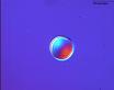 |
Figure:
1. Light microscopy image of single pulse ablated Si surface.
2. Light microscopy image of single pulse ablated Si surface at a lower fluence.
|
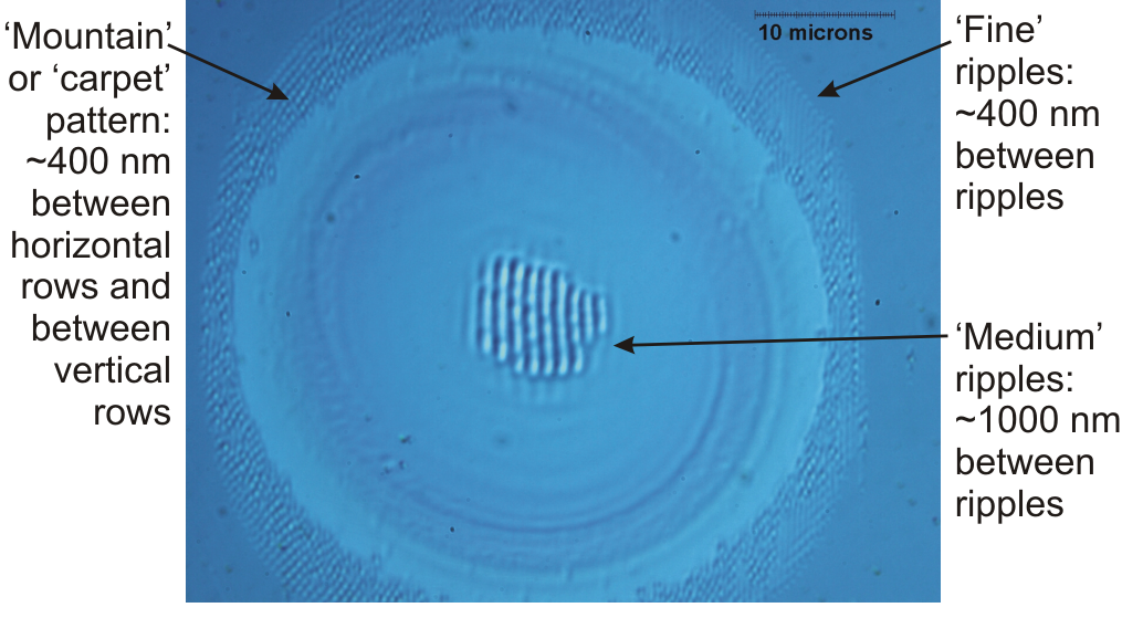
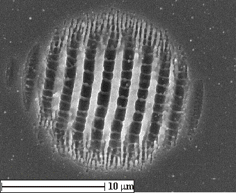
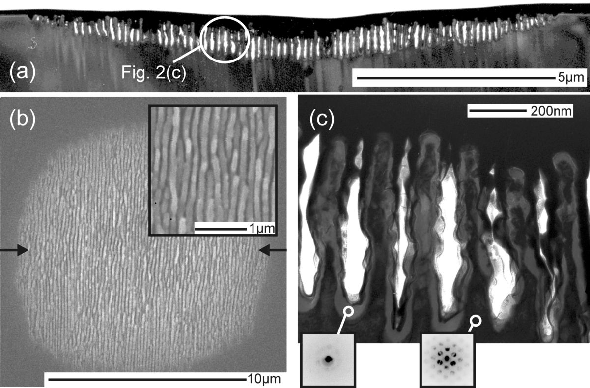
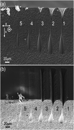
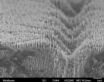
Irradiation of samples with multiple pulses leads to interesting
surface structuring effects, such as the formation of laser
induced periodic surface structures (LIPSS). Figures below
show formation of such structures on various semiconductor
surfaces. (Click to enlarge the images.)
| Femtosecond Micromachining |
Many practical laser applications involve cutting, drilling
and scribing. We investigate the ablation rates, morphology,
geometry as well as collateral damage caused by laser micromachining. (Click to enlarge the images.)
| 1 |
 |
2* |
 |
3 |
 |
| 4 |
 |
5 |
 |
6 |
 |
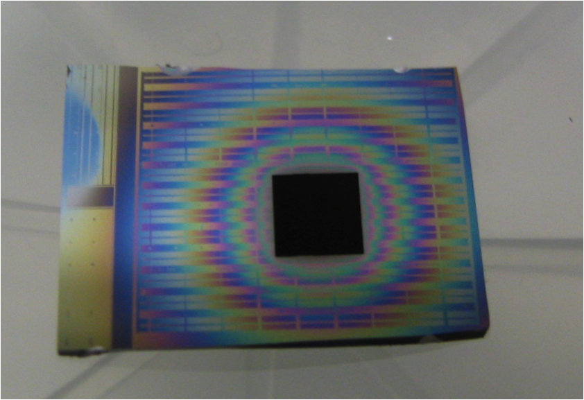
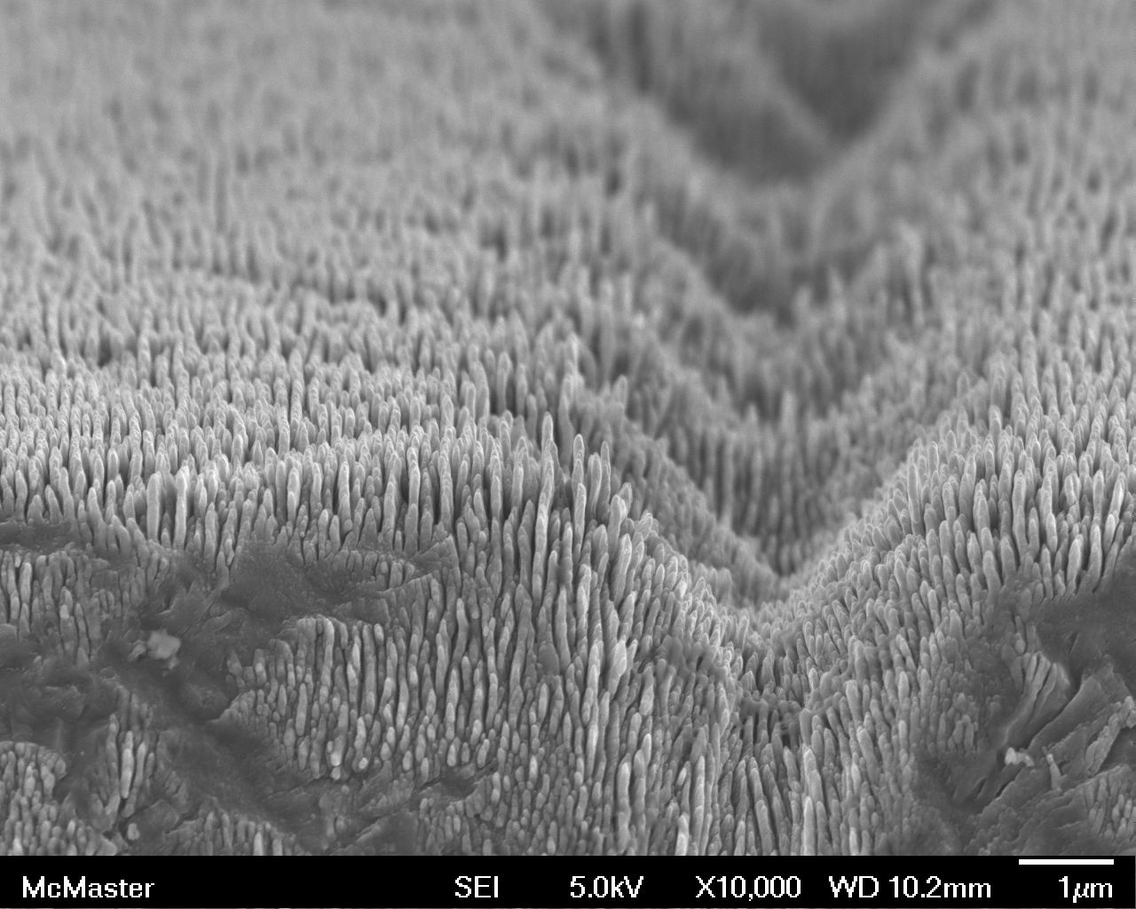
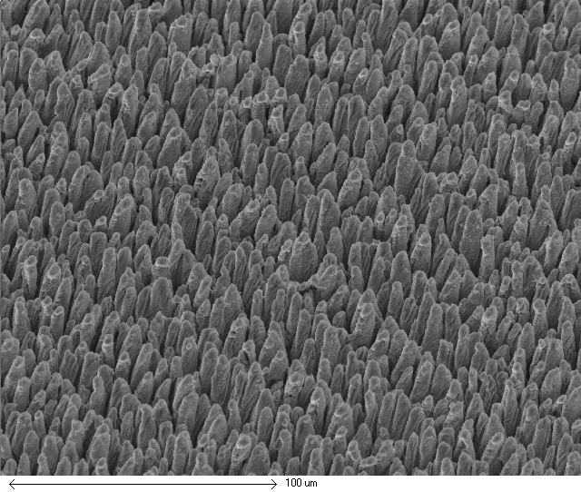
Figure:
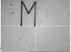
1. McMaster Engineering Logo micromachined on Si surface. The MPEG clip shows
diffraction effects after illumination of the pattern with white light at various angles.
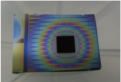
2*. SEM images of the side and top surfaces of grooves micromachined in diamond. The laser beam was focused into the bulk
and scanned across the polished surface out of a rough side edge.
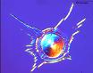
3. Microstructuring of Si surface (black area) on prepatterned SiO2-on-Si sample. Deposition
of ejected nanoparticles form the colour rings.
4. MPEG clip of laser writing.
5. SEM image of pointed structures on diamond. Machining conditions were similar to that of Figure 2.
6. Microstructured Si surface.
|
Please Note: Some of the images used in this page have been published and are protected by copyright. Please contact us
before reusing the images.
+This image appeared in APL 92, 221112 (2008) and may be found here. Copyright (2008) American Institute of Physics. This article may be downloaded for personal use only. Any other use requires prior permission of the author and the American Institute of Physics.
*This image appeared in APA 103, 185 (2011) and may be found springerlink.com.
| 


 Back to Top